Thursday, December 31, 2020

Characteristics(Parameters) of an Op-Amp - Definitions, Equivalent Circuit

Characteristics of Op-Amp 

The characteristics of Op-Amp is very important because we can compare the performance of various Op-Amp ICs and select the best suitable Op-Amp for any desired application.

Equivalent Circuit of an Op-Amp 


The characteristics of an Op-Amp are divided into two types namely AC characteristics and DC characteristics. The AC characteristics include the frequency response, frequency compensation, Bandwidth, slew rate, and stability of Op-Amp whereas the DC characteristics include input offset voltage, the input offset current, input bias current, and thermal drift, etc.

Let’s understand each characteristic one by one. 

Open Loop Voltage Gain

Open-loop voltage gain is defined as the differential gain of an Op-Amp in the open-loop mode of operation. Note that open-loop mode is the mode of operation without any feedback. The open-loop gain is very high. It is denoted by AV.

Input Offset Voltage

The input offset voltage is defined as a small differential voltage that is applied at the input of the Op-Amp to make the output voltage zero. It is denoted by Vios.

Ideally, the output voltage of an Op-Amp should be zero for a zero-input voltage. But practically, due to unbalancing in the differential input stage of the Op-Amp, the output is not zero. So, we have to apply a small differential voltage at the input stage of the Op-Amp to make the output voltage zero.

The value of input offset voltage is temperature-dependent and it is about a few mV ranges. 

Output Offset Voltage

The output voltage produced due to input offset voltage is called output offset voltage. It is denoted by Voos

Input Offset Current

Input Offset Current is defined as the algebraic difference between current flowing into the inverting and non-inverting terminals of the Op-Amp. It is denoted by Iios.

Mathematically, it can be expressed as 

Input Bias Current

Input Bias Current is defined as the average value of the current flowing into the inverting and non-inverting terminals of the Op-Amp. As shown in the figure, the current flowing into non-inverting input is IB2 and the current flowing into inverting input is IB1.

Hence, the input bias current is given by

The value of input bias current is temperature-dependent and it should be as low as possible. 

Differential Input Resistance

Differential Input Resistance is defined as the equivalent resistance which can be measured at either the inverting or non-inverting input terminal of the Op-Amp with the other terminal connected to the ground. It is also called the input resistance of the Op-Amp. It is denoted by Ri.

The value of differential input resistance should be as high as possible. It is about a few M for the Op-Amps if a transistor is used as an input and about to GΩ for the Op-Amps if FET is used as an input.

Output Resistance

Output Resistance is defined as the resistance which can be measured at the output terminal of the Op-Amp with input short-circuited.

The value of the output resistance should be as small as possible because it improves the output voltage regulation and current sourcing capacity.

CMRR

CMRR stands for Common Mode Rejection Ratio is defined as the ratio of differential gain to common-mode gain. It is denoted by ƿ.

Mathematically CMRR can be expressed as,  


In decibels, CMRR can be expressed as,

CMRR is the ability of the Op-Amp to reject the common-mode signal successfully. Hence, it is the figure of merit of the Op-Amp.

Ideally, the value of CMRR should be infinite and practically it should be as high as possible. Higher the value of CMRR means better the ability of Op-Amp to reject the noise. 

PSRR

PSSR stands for Power Supply Rejection Ratio is defined as the change in input offset voltage of an Op-Amp due to the change in the supply voltage of an Op-Amp. It is also known as the Supply Voltage Rejection Ratio (SVRR) or Power Supply Sensitivity (PSS).

Mathematically PSRR can be expressed as,  

Ideally, the value of PSRR should be zero and practically it should be as small as possible.

Slew Rate

The Slew Rate of an Op-Amp is defined as the maximum rate of change of output voltage per unit time. It is expressed in Volts/microseconds.

Mathematically PSRR can be expressed as,  

Bandwidth

The bandwidth of the Op-Amp is the range of frequencies over which all the signal frequencies are amplified equally.

The bandwidth of an Op-Amp should be capable of amplifying the signals from 0 Hz frequency. It should be as large as possible. 

Gain Bandwidth Product

Gain Bandwidth Product is defined as the bandwidth of Op-Amp when the voltage gain is unity (1). It is also called unity-gain bandwidth or small signal bandwidth.


Thursday, December 17, 2020

Op-Amp (Operational Amplifier) - Definition, Symbol and Terminals

 What Is an Op-Amp?

An Op-Amp stands for an operational amplifier is defined as a multistage amplifier in which a number of amplifier stages are interconnected to each other. In other words, the Op-Amp is basically a voltage amplifier with a high voltage gain. The term Op-Amp or operational amplifier was first used by John R. Ragazzini in the year of 1947.

An Op-Amp can be used to perform a variety of operations like addition, subtraction, differentiation, integration, and amplification.

The popular Op-Amp IC is 741 Op-Amp IC. The typical gain of a 741 Op-Amp is 2 * 105 or 106 dB. 

Symbol and Terminal of 741 Op-Amp

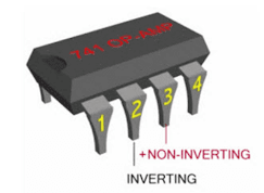
The physical appearance and the circuit symbol of a 741 Op-Amp are shown in the below figure.

Physical Appearance

As shown in the above figure, an Op-Amp has two input terminals, one output terminal, and two supply voltage terminals.

Input of an Op-Amp

An Op-Amp has two input terminals, one input is called inverting input which is marked as a negative sign (-) and the second input is called non-inverting input which is marked as a positive sign (+). We can apply the input voltage which is to be amplified to any one of the above inputs and another pin is connected to the ground.

If we connect the input signal to the inverting terminals then we get the amplified output signal which is 1800 out of phase with the input signal. Hence, it is known as an inverting input. Similarly, if we connect the input signal to the non-inverting terminals then we get the amplified output signal which is in phase with the input signal. Hence, it is known as a non-inverting input. It is shown in the below figure.  

Input and Output Signal with 1800 Inverted Output and Non-Inverted Output When Input Signal is Applied to the Inverting and Non-Inverting Terminal of an Op-Amp     


DC Power Supply for an Op-Amp

The dual polarity power supply is necessary for the operation of an Op-Amp. Here, the +VCC and -VEE are the power supply terminals of the Op-Amp. The +VCC terminals of an Op-Amp are connected to the positive terminal of the one source and the -VEE terminal of an Op-Amp is connected to the other source as sown in the below figure.


 The Op-Amp 741 IC needs a dual polarity power supply as shown in the figure. However, there are some other Op-Amps that can operate on a single polarity supply.


Wednesday, December 9, 2020

Power Factor - Definition, Formula, Disadvantages of Low Power Factor

What is Power Factor?

Definition 1: Power Factor is defined as the cosine angle between the voltage and the current. 

Definition 2: Power Factor is defined as the ratio of the active power to the apparent power.


Definition 3: Power Factor is defined as the ratio of the resistance to the impedance.
 

Disadvantages of Low Power Factor

The power factor plays an important role in A.C. circuits as power consumed in A.C. circuits is depending on the power factor.

    Now, we know that the current in a single-phase circuit is given by  

and the current in a three-phase circuit is given by  


It is clear from the above equation that for a fixed amount of power and voltage, the load current is inversely proportional to the power factor. Hence, for the smaller power factor, the higher is the load current and for the higher load factor, the smaller is the load current. The large current due to low power factor results in the following disadvantages. 

(i)               Greater Conductor Size: 

To transmit and distribute a given amount of power at a constant voltage, the conductor will have to carry more current at a low power factor. Hence, the greater size of the conductor required to carry more current. 

(ii)             Large kVA rating of the equipment: 

In an electrical circuit, the electrical equipment i.e., alternators, transformers, motors, switchgear, etc., are always rated in kVA.

Now, 

Hence, it is clear from the above equation that the kVA rating of the equipment is inversely proportional to the power factor. Thus, for the smaller power factor, the larger the kVA rating and for the larger power factor, the smaller the kVA rating. Therefore, at a low power factor, the kVA rating of the equipment has to be made larger, making the equipment larger and more expensive.  

(i)               Large copper losses:

The large current at low power factor causes increased I2R losses in all the equipment. This results in poor efficiency.

 (iii)         Poor voltage regulation: 

The large current at low power factor causes greater voltage drops in transformers, alternators, motors, transmission lines, and distribution lines. Hence, reduced voltage available to the utilization devices which impacts their performance. For example, due to reduced voltage, the starting torque of the motors is reduced, lightning becomes dimmer, etc. To maintain the required voltage within permissible limits, the voltage regulator is required.  

Friday, December 4, 2020

Per Unit Value (What Is It?) - Formula, Example, Advantages


Per Unit Value – What Is It?

Per Unit Value of a quantity is defined as the ratio of the actual value of that quantity to an arbitrarily selected value of that quantity. This arbitrarily selected value is known as the base value. The per-unit value is dimensionless because the actual value and base value both are expressed in the same units.


Per Unit Impedance Calculation at a New Base Value - Formula

The per unit impedance is defined as the ratio of the actual impedance to the base impedance.


In 3 phase-systems the base values are usually selected based on 3-phase kVA and line to line kV. Then,

 Put the value of base current into the above equation we get,

For a circuit containing transformers, it is convenient to select the base kVA for both sides of transformers. However, the ratio of base voltages on the two sides is kept the same as the transformation ratio. Such a selection gives the same per unit impedance on either side of the transformer.

It is usually necessary to transform the per unit impedance from one set of base values to a new set of base values. This can be done by using the following equation. 

Let’s see examples of how to calculate per unit impedance at a new base value by using  the     above equation. 

Example: The per-unit impedance of an alternator corresponding to base value 13.3 kV and 20 MVA is 0.2 p.u. calculate p.u. value of the impedance for base values of 13.9 kV and 40 MVA in p.u?

Solution:

Given Data:                     Z(old) = 0.2 p. u

               Base kV(old) = 13.3 kV

              Base kV(new) = 13.9 kV

           Base MVA (old) = 20 MVA

          Base MVA (new) = 40 MVA

Now, the formula to calculate impedance at a new base value is given by,


Advantages of a Per Unit System 

Some of the advantages of a per-unit system are listed below.

  • Manufactures generally specify the impedance values of equipment’s in a per unit of the equipment’s rating. If any information is not available then it is easy to figure its per unit value than its numerical value. 

  • The power system contains a large number of transformers. The ohmic value of an impedance is referred to the secondary is different from the value as referred to the primary. Although, if the base values are selected properly, the per-unit impedance is the same on both the sides of the transformer. 

  • The transformer connections in 3-phase circuits do not affect the per-unit value of impedance although the base voltage on two sides depends on the connections.

  • When parameters expressed in a per unit value then it is tending to fall in relatively narrow numerical ranges. Hence, any erroneous data can be easily identified. 

  •  Per unit value represents yields important information about relative magnitudes. 


Thursday, December 3, 2020

Comparison Between RTD and Thermocouple


The comparison between RTD and Thermocouple is listed in the below table.

Parameter

RTD

Thermocouple

Principle of operation

Resistance changes with temperature

The voltage is induced proportional to temperature

Type of transducer

It is a Passive type transducer hence dc source is required for its operation.

It is an Active type transducer hence external dc source is not required for its operation.

Temperature range

-2000 C to 6500 C

-2000 C to 11000 C

Sensitivity

Excellent

Good

Response time

Good

Excellent

Cost

High

Moderate

Accuracy

Very good

Moderate

Size

Large

Small

Material used

Platinum, Nickle, Copper, Semiconductors, etc.

Iron-constantan, Copper-constantan, etc.

Linearity of characteristics

Non-linear

Non-linear

Compensation

Not required

Cold junction compensation is required

Applications

For shorter temperature range applications

For wide temperature range applications


RTD


Thermocouple

Analog and Digital Instruments - What they Are? (Comparison and Advantages of Digital Instruments over Analog Instruments)

Analog and Digital Instruments What are Analog Instruments? The signals which continuously vary and take infinite values for a given range a...